Anodic bonding is a wafer bonding process to seal glass to either silicon or metal without introducing an intermediate layer. It is commonly used to seal glass to silicon wafers in electronics and microfluidics. This procedure is mostly used for hermetic encapsulation of micro-mechanical silicon elements.
What Can be Done with Anodic Bonding?
Anodic bonding, a wafer bonding process, is primarily used to hermetically seal glass to silicon or metal, especially in electronics and microfluidics. This process enables the creation of durable, leak-tight connections between these materials, which is crucial for various applications.
- Encapsulation of MEMS devices: Anodic bonding allows for the encapsulation of micro-mechanical silicon elements within a sealed glass structure, protecting them from environmental factors.
- Microfluidic channels and systems: Sealing glass to silicon or metal allows for construction of microfluidic devices with precise and reliable fluid handling.
- Creating reliable seals for integrated circuits: Anodic bonding helps to create reliable and robust seals for integrated circuits, ensuring long-term performance and reliability.
- Generating hermetic enclosures: Anodic bonding can create hermetic enclosures, which are completely sealed and airtight, for various electronic components.
- Joining different materials: It enables the joining of different materials, such as glass and silicon, with minimal stress and good adhesion.
- Creating 3D structures: In some cases, anodic bonding is used to create 3D structures by stacking multiple layers of materials together.
In essence, anodic bonding provides a reliable and versatile method for creating durable connections between glass and other materials, enabling a wide range of applications in electronics, microfluidics, and other fields.
What are the Benefits of Anodic Bonding?
Anodic bonding offers several advantages, including creating strong, hermetic seals without requiring an interlayer. This process allows for joining silicon and glass, or other materials, while maintaining the integrity of structures and minimizing parasitic capacitance. It also enables precise alignment, optical addressing, high yields, and tolerance to surface imperfections. Optical addressing refers to directing light beams to specific locations or individual quantum objects, like trapped ions, to control their behavior.
Strong and Hermetic Seals
- Anodic bonding forms a strong, permanent bond between the bonded materials.
- The process creates a hermetic seal, effectively preventing gas leakage and environmental contamination.
- The seal forms in a vacuum or a controlled atmosphere, allowing for the encapsulation of gases or the creation of sealed cavities.
No Interlayer Required
- Unlike other techniques, anodic bonding doesn’t require an intermediate layer.
- This simplifies the process and reduces the possibility of interlayer defects.
Minimal Pressure and Low Bonding Temperature
- The electrostatic fields in anodic bonding allow you to apply minimal force, making it suitable for fragile components.
- The relatively low bonding temperature (typically below 450°C) provides greater design flexibility and avoids unwanted structural changes.
Maintains Structure Integrity
- Anodic bonding can seal around grooves, cavities, and other structures without losing dimensional tolerances.
- This ensures that the bonded materials maintain their original shape and dimensions.
Minimal Parasitic Capacitance
- Since glass is an electrical insulator, anodic bonding minimizes parasitic capacitances, which can affect the performance of electronic devices.
High Yield and Tolerance to Imperfections
- Anodic bonding is tolerant to surface contamination and wafer warpage, making it a high-yield process.
- The electrostatic force helps overcome these surface irregularities, ensuring a reliable bond.
Enables Complex 3D Structures
- Anodic bonding can create multi-layer stacks, enabling the fabrication of complex 3D microstructures.
Precise Alignment and Optical Addressing
- The transparency of glass at visible wavelengths allows for simple and accurate alignment of pre-patterned wafers.
- Exploit this transparency for optical addressing and viewing of microfluidic devices.
Low Cost and Scalable
- You can perform anodic bonding on a wafer scale, offering a low-cost process for first-order packaging.
Versatile Material Joining
- This type of bonding can join various materials, including silicon, glass, and metals, without needing an intermediate layer.
What is the Strength of Anodic Bonding?
Anodic bonding offers several advantages, including creating strong, hermetic seals without requiring an interlayer. This process allows for joining silicon and glass, or other materials, while maintaining the integrity of structures and minimizing parasitic capacitance. It also enables precise alignment, optical addressing, high yields, and tolerance to surface imperfections. Optical addressing refers to directing light beams to specific locations or individual quantum objects, like trapped ions, to control their behavior
The typical strength is between 10 and 20 MPa. This, according to pull tests, is higher than the fracture strength of glass. That is why differing coefficients of thermal expansion pose challenges for anodic bonding.
How Does Anodic Bonding Work?
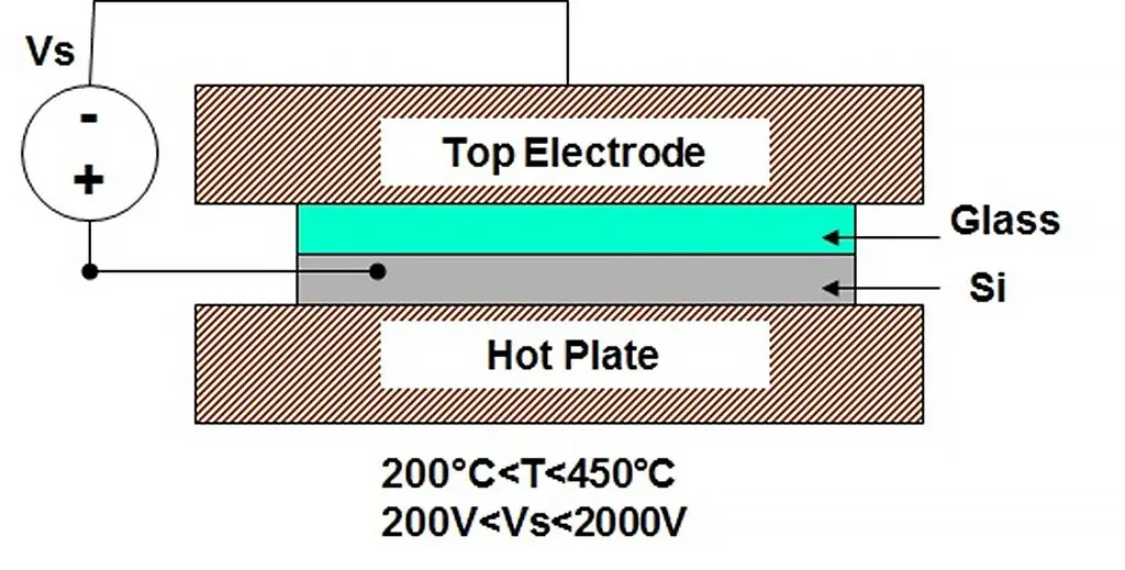
Anodic bonding is a hermetic seal between two materials through an electrostatic field at elevated temperature, and occurs between glass-glass, silicon-glass, and silicon-quartz interfaces. The method is mostly to bond alkali ion-rich glass (borosilicate or pyrex glass) and a semiconductor or metal.
Does Anodizing Add Thickness?
Yes, anodizing typically adds thickness to a metal part. The anodized layer grows both outward and inward into the metal, creating a layer that’s thicker than the original surface. The 50-50 rule generally applies, meaning about half the layer’s thickness is outward growth and half is ingress into the material.
Anodizing creates a layer of aluminum oxide on the surface of aluminum (and other metals) through an electrochemical process. Therefore, this aluminum oxide layer is thicker than the original aluminum surface, adding to the overall dimensions of the part.
The anodized layer’s growth is not just a surface buildup. It penetrates slightly into the metal. Therefore, the thickness is approximately split outward (growth) and inward (ingress). You can control the thickness of the anodized layer by adjusting the current density and the time spent in the anodizing bath.
The increase in thickness due to anodizing can be a significant factor in dimensional tolerances, especially for parts with tight fits or critical dimensions.
Learn more about the anodic bonding process at Precision Glassblowing by contacting us by email or by phone.